Borofloat 33 Glass Substrate Engineered for Excellence in High-Tech
Applications and Precision Operations
Borofloat 33® Glass Substrates: Precision, Durability, and
Versatility Redefined
Unlock next-level performance for your high-tech applications with
Borofloat 33® Glass Substrates, the borosilicate glass engineered
for extreme thermal, chemical, and mechanical resilience. Renowned
for its ultra-low thermal expansion and superior surface quality,
Borofloat 33® is the go-to choice for industries demanding
precision under stress.
Why Borofloat 33® Stands Out
- Exceptional Thermal Stability: Withstand rapid temperature swings
(-60°C to 450°C) without distortion, thanks to its near-zero
thermal expansion (CTE: 3.25 × 10⁻⁶/K).
- Optical Clarity & Chemical Resistance: High transmission from UV
to IR (280nm–2,000nm), paired with resistance to acids, alkalis,
and solvents, ensures longevity in harsh environments.
- Flame-Polished Surface Perfection: Achieve minimal surface
roughness (≤1nm Ra) and pristine flatness, critical for MEMS,
microfluidics, and thin-film coatings.
- Customizable Solutions: Available in thicknesses (0.3mm to 15mm),
sizes up to 1,100mm × 1,450mm, and post-processing options
(chemically strengthened, etched, or drilled).
Applications That Demand Excellence
From semiconductor wafer carriers and precision optics to
lab-on-a-chip devices and high-power LED encapsulation, Borofloat
33® empowers innovation across:
- Electronics: RF/microwave substrates, hermetic packaging
- Biotech: Microfluidic chips, biosensor platforms
- Energy: Solar panel covers, fuel cell components
- Industrial: High-temperature viewports, laser system optics
Borofloat 33 Glass Wafer Parameters
| Material | BOROFLOAT 33 |
| Density (@ 25°C/77°F) | 2.23 g/cm3 |
| Modulus of Elasticity | 63 kN/mm2 |
| Knoop Hardness HK 0.1/20 | 480 |
| Poisson’s Ratio | 0.2 |
| Dielectric Constant (@ 1 MHz & 25°C) | 4.6 |
| Loss Tangent (@ 1 MHz & 25°C) | 37 x 10-4 |
| Dielectric Strength(@ 50 Hz & 25°C) | 16 kV/mm |
| Refractive Index (nd) | 1.472 |
| Dispersion (nF - nC) | 71.9 x 10⁻⁴ |
Borofloat 33 Glass Wafer Specifications
| Specification | 3” | 4” | 5" | 6" | 8" |
| Diameter | 76.2mm | 100mm | 125mm | 150mm | 200mm |
| Tol(±) | <0.1~0.25 mm |
| Thickness | >0.10mm | >0.10mm | >0.30mm | >0.30mm | >0.30mm |
| Primary Flat | 22mm | 32.5mm | 42.5mm | 57.5mm | Notch |
| Notch |
| TTV | <8um | <10um | <15um | <20um | <30um |
| Bow | ±20um | ±25um | ±40um | ±40um | ±60um |
| Warp | <30um | <40um | <50um | <50um | <60um |
| PLTV(<0.5um) | ≥95%(5mm*5mm) |
| Transmittance | UV, Optical, IR or Custom option |
| Edge Rounding | Compliant with SEMI M1.2 Standard/refer to IEC62276 |
| Surface Type | Single Side Polished /Double Sides Polished |
| Polished side Ra | <1.0nm or specific per requested |
| Back Side Criteria | General is 0.2-0.5µm or as customized |
| Appearance | Contamination | None |
| Particles>0.3µm | <=30 |
| Saw Marks, striations | None |
| Scratch | None |
| Cracks, saw marks, stains | None |
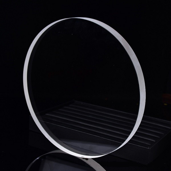
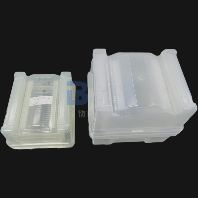
Glass Wafer Photos


FAQs:
- Q: What are the products you mainly work on?
A: We look at ourselves as the piezo wafer specialist. We are the
very first to work with Single Crystal Quartz in China about 30
years ago. Then gradually we step in the field of LiNbO3, LiTaO3,
Quartz glass, LGS, CTGS etc. Especially, if you are looking for a
piezo quartz supplier, we are the ultimate choice! We export
millions of quartz blanks each year because we master the AT, SC
and IT cuts with superior angle precision.
- Q: Can you accept product customization?
A: Yes, of course. We can fabricate as per your request. In addition,
we are so experienced with piezo wafers that we can provide you
relevant suggestions if you are not 100% sure about your choice.
Besides, we do have some standard wafers in stock, please check
with us.
- Q: Can you deliver the goods via our courier agent?
A: Yes, we would suggest you go with the courier agent you are most
familiar with (DHL, FedEX, UPS etc.). We can ship via your account.
And, of course, we will pack the products safely in acceptable size
to help you save the shipping cost. If you need us to take care of
the freight, it’s also not a problem. We also have good discount
with the international courier companies.
- Q: How can you guarantee we get what we want safely?
A: The wafer products are fragile and sometimes expensive. The last
thing, as the manufacturer, we want to see is the products we make
were damaged during courier. As a result, we will pack the wafers
adequately and put them in a proper carton filled with buffer
sponge. However, accidents are inevitable sometimes. So, please
follow the “Acceptance check” steps shown in the drawings below. If the unwanted happened, we
will either give the replenishment or refund if you follow the
checking steps.
- Q: Can we visit your factory?
A: Sure. Factory inspection is important for large quantity purchase
and long-term cooperation. Face to face discussion is what we
mostly confident with. During the past years, big names around the
world have witnessed our progress in factory build-up. These days,
due to the Covid-19 pandemic, we also had the experience of
videoconferencing with global buyers.
Acceptance Check
- The product is fragile. We have adequately packed it and labeled it
fragile. We deliver through excellent domestic and international
express companies to ensure transportation quality.
- After receiving the goods, please handle with care and check
whether the outer carton is in good condition. Carefully open the
outer carton and check whether the packing boxes are in alignment.
Take a picture before you take them out.
- Please open the vacuum package in a clean room when the products
are to be applied.
- If the products are found damaged during courier, please take a
picture or record a video immediately. DO NOT take the damaged
products out of the packaging box! Contact us immediately and we
will solve the problem well.


