| Sign In | Join Free | My himfr.com |
|
| Sign In | Join Free | My himfr.com |
|
| Ask Lasest Price | |
| Brand Name : | BonTek |
| Model Number : | Lithium Tantalate (LiTaO3) |
| Certification : | ISO:9001, ISO:14001 |
| Price : | Negotiable |
| Payment Terms : | T/T |
| Supply Ability : | 10000 pcs/Month |
| Delivery Time : | 1-4 weeks |
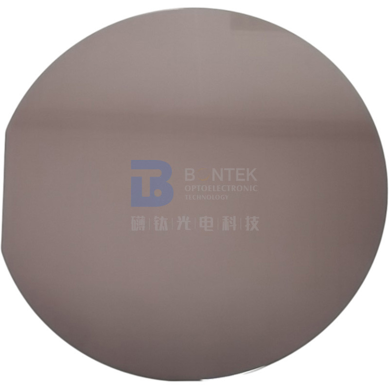
Compound Semiconductors LiTaO3 Wafer used for several Optical Devices, SAW Devices
Compound semiconductors are the semiconductors composed of more than two chemical elements. Lithium Tantalate(LiTaO3) wafer is used for several optical devices, especially surface acoustic wave(SAW) device. Because of the lithography in SAW device process, LiTaO polishing is needed. In this paper, the commercial slurries(NALCO2371^(TM), ILD1300^(TM), ceria slurry) used for chemical mechanical polishing(CMP) were tested, and the most suitable slurry was selected by measuring material removal rate and average centerline roughness(Ra). From these result, it was proven that ILD1300^(TM) was the most suitable slurry for LiTaO wafer CMP due to the chemical reaction between solution in slurry and material.


Diameter | Orientation | Thickness | Primary Flat | Material | Brand /Grade |
76.2±0.2mm | 36°Y Cut | 0.5±0.025mm | 22±2mm | LiTaO3 | SAW |
76.2±0.2mm | 36°Y Cut | 0.5±0.025mm | 22±2mm | Black LiTaO3 | SAW |
76.2±0.2mm | 42°Y Cut | 0.5±0.025mm | 22±2mm | LiTaO3 | SAW |
76.2±0.2mm | 42°Y Cut | 0.5±0.025mm | 22±2mm | Black LiTaO3 | SAW |
76.2±0.2mm | X-112°Y Cut | 0.5±0.025mm | 22±2mm | LiTaO3 | SAW |
76.2±0.2mm | X-112°Y Cut | 0.5±0.025mm | 22±2mm | Black LiTaO3 | SAW |
76.2±0.2mm | X Cut | 0.5±0.025mm | 22±2mm | LiTaO3 | Optical |
76.2±0.2mm | Z Cut | 0.5±0.025mm | 22±2mm | LiTaO3 | Optical |
100±0.2mm | 36°Y Cut | 0.5±0.025mm | 32±2mm | LiTaO3 | SAW |
100±0.2mm | 36°Y Cut | 0.5±0.025mm | 32±2mm | Black LiTaO3 | SAW |
100±0.2mm | 42°Y Cut | 0.5±0.025mm | 32±2mm | LiTaO3 | SAW |
100±0.2mm | 42°Y Cut | 0.5±0.025mm | 32±2mm | Black LiTaO3 | SAW |
100±0.2mm | X-112°Y Cut | 0.5±0.025mm | 22±2mm | LiTaO3 | SAW |
100±0.2mm | X-112°Y Cut | 0.5±0.025mm | 22±2mm | Black LiTaO3 | SAW |
100±0.2mm | X Cut | 0.5±0.025mm | 22±2mm | LiTaO3 | Optical |
100±0.2mm | Z Cut | 0.5±0.025mm | 22±2mm | LiTaO3 | Optical |
Chemical formula | LiTaO3 |
Molar mass | 235.887 g/mol |
Density | 7.46 g/cm3, solid |
Melting point | 1,650°C (3,000°F; 1,920K) |
Solubility in water | Insoluble in water |
Crystal structure | Space group R3c |
Lattice constant | a = 515.43 pm, c = 1378.35 pm |


FAQs:
A: We look at ourselves as the piezo wafer specialist. We are the very first to work with Single Crystal Quartz in China about 30 years ago. Then gradually we step in the field of LiNbO3, LiTaO3, Quartz glass, LGS, CTGS etc. Especially, if you are looking for a piezo quartz supplier, we are the ultimate choice! We export millions of quartz blanks each year because we master the AT, SC and IT cuts with superior angle precision.
A: Yes, of course. We can fabricate as per your request. In addition, we are so experienced with piezo wafers that we can provide you relevant suggestions if you are not 100% sure about your choice. Besides, we do have some standard wafers in stock, please check with us.
A: Yes, we would suggest you go with the courier agent you are most familiar with (DHL, FedEX, UPS etc.). We can ship via your account. And, of course, we will pack the products safely in acceptable size to help you save the shipping cost. If you need us to take care of the freight, it’s also not a problem. We also have good discount with the international courier companies.
A: The wafer products are fragile and sometimes expensive. The last thing, as the manufacturer, we want to see is the products we make were damaged during courier. As a result, we will pack the wafers adequately and put them in a proper carton filled with buffer sponge. However, accidents are inevitable sometimes. So, please follow the “Acceptance check” steps shown in the drawings below. If the unwanted happened, we will either give the replenishment or refund if you follow the checking steps.
A: Sure. Factory inspection is important for large quantity purchase and long-term cooperation. Face to face discussion is what we mostly confident with. During the past years, big names around the world have witnessed our progress in factory build-up. These days, due to the Covid-19 pandemic, we also had the experience of videoconferencing with global buyers.
Acceptance Check

|
|


